Scientific breakthroughs begin at the Joint School of Nanoscience and Nanoengineering (JSNN). As part of its mission to forge partnerships with scientists in industry, academia, and government, JSNN established the Joint School’s Institute for Research Technologies (JSIRT). This core research facility provides advanced scientific instrumentation for researchers across North Carolina and beyond.
Research instruments often come with a hefty price tag. As a shared-user facility, JSIRT provides fee-for-use access to advanced microscopy, flow cytometry, electron-beam lithography, materials characterization, and computational research tools. This technology offers unique opportunities for JSNN students, UNCG researchers, and external academic and industry partners.
“JSIRT makes advanced research more accessible by connecting students, faculty, and industry partners with sophisticated tools and the expertise to use them effectively,” says Dr. Shyam Aravamudhan, nanoengineering professor and director of JSIRT.
For JSNN students, the hands-on experience they gain with advanced research instruments prepares them for a wide range of career opportunities, whether in academia, industry, or government, or if they pursue entrepreneurship.
Flow Cytometry Expands Access to Advanced Cell Analysis
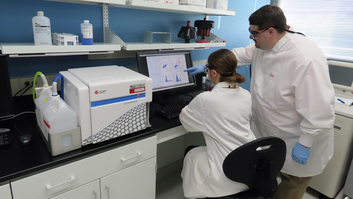
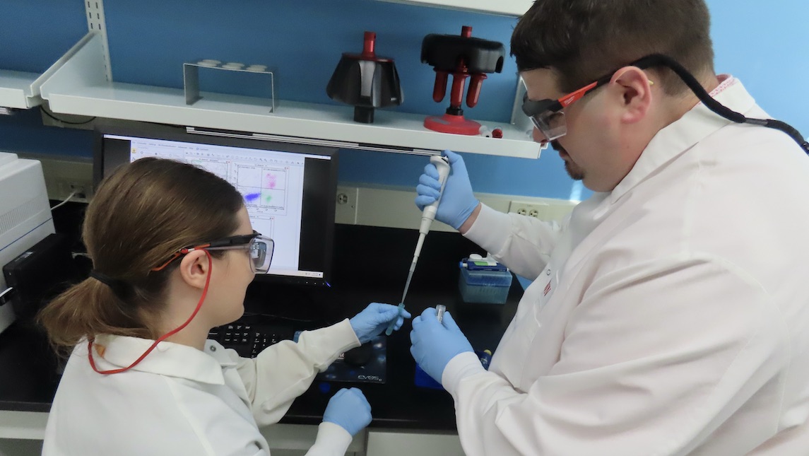
The Beckman CytoFLEX Flow Cytometer is a highly sophisticated cell counter and sorter; it rapidly analyzes thousands of cells per second. The instrument records information about each cell’s size, its complexity, and any fluorescent tags attached to it, enabling researchers to access a significant amount of detail from every cell in a single experiment.
Flow cytometry functions by passing cells in a stream of buffered liquid through an optics path at extremely high speeds. The optics path allows users to detect a large number of fluorescent tags all at once. The fluorescent tags allow different cells to be identified and measured. This technology helps researchers study cell health, immune responses, and genetic modifications.
JSNN students and faculty heaviy use the flow cytometer, and it supports projects involving UNCG, N.C. A&T State University, and external academic partners. In fact, two-thirds of JSNN biology labs use flow cytometry in their research, according to Biology Lab & EHS Technician Luke Dixon, MESH.
External users can also benefit. “Flow cytometry is an expensive technique, and small companies often rely on access to JSIRT’s maintained, professionally staffed instrumentation to conduct research and be productive,” says Dr. Steven Crawford, equipment manager.
Scanning Electron Microscopy Reveals the Nanoscale World
The JEOL IT-800 SEM/EDX, a high-resolution scanning electron microscope (SEM), enables users to see much smaller objects with finer detail. High magnifications with light microscopes are on the order of 1,000x, but SEM works at magnifications of 100,000x or greater. Researchers also use SEM for lower-magnification work because it provides exceptional depth of field and contrast for a 3D appearance and determines a specimen’s elemental composition.
The capabilities of the SEM are important because most viruses, some subcellular components, state-of-the-art electronics, natural and engineered nanomaterials, and countless other phenomena are not resolvable with light microscopes. Therefore, powerful imaging capabilities are needed to see the world at the nanoscale, in order to advance knowledge, science, and technology.
JSIRT is the only location in the Triad offering open access to the SEM for external academic and industry clients. Alongside traditional scientific and engineering academic research, it also hosts partners from many industries, including textiles, electronics, polymers, life sciences, and others.
“With more than 100 operators and 100 projects utilizing this SEM, we host training sessions most weeks throughout the year,” says Dr. Kyle Nowlin, a nanoscience senior research scientist. “Over the past decade, we have trained hundreds of SEM users, most of whom are graduate students.”
JSNN faculty are also active SEM users. The labs of Dr. Dennis LaJeunesse and Aravamudhan use SEM to investigate how microorganisms interact with nanoscale materials. Dr. Suzanne Ahmed uses the instrument to characterize segmented multi-metallic nanorobots, visualizing their form, structure, and elemental properties.


Electron-Beam Lithography Brings Nanoscale Fabrication Within Reach
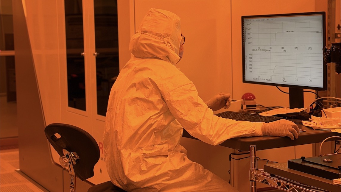
Similar to using a stencil to create a design, lithography produces exceptionally small patterns needed for electronic chips. Normally, light is used in lithography, but its wavelength limits pattern size, making it challenging to create nanoscale features. Instead of light, JSIRT offers an electron beam.
“The Raith Voyager E-beam Lithography System is an advanced tool designed to produce highly precise nanoscale patterns for applications such as nanoelectronics, semiconductors, quantum devices, sensors, photonics, and other areas of nanotechnology,” says Dr. Binod Rizal, a nanoengineering research scientist.
Researchers currently use the system to fabricate devices based on two-dimensional materials and patterns for nanowire-based single-photon detectors.
A recent addition to JSIRT, the Raith Voyager is available to internal and external users. It supports local micro- and nanotechnology research institutes, universities, and companies by providing both on-site and remote access to advanced nanoscale fabrication capabilities.
Supporting the Science Behind Smarter Materials
From smartphones and cars to batteries and medical devices, engineered materials need to be safe, strong, and reliable. Because a material performance often depends on how its outer surface interacts with the environment, scientists need tools that can examine that boundary in exceptional detail.
“Standard testing only gives a high-level overview,” says Dr. Shobha Mantripragada, a nanoengineering research associate. “Scientists need to zoom in closer to identify the specific ‘body parts’ or functional groups that dictate how the surface behaves.”
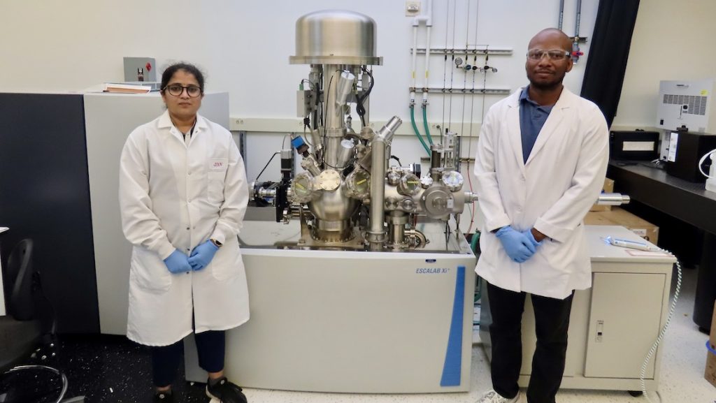
X-ray Photoelectron Spectroscopy (XPS), a surface-analysis instrument, can zoom in on the outermost material layer to identify distinct chemical features. By directing X-rays at a material and measuring the energy of the electrons knocked free, XPS reveals the exact elements and chemical bonds present within the top few layers.
The instrument is invaluable for inspecting protective coatings, detecting contamination, and analyzing corrosion, enabling researchers to troubleshoot product failures and develop next-generation technologies.
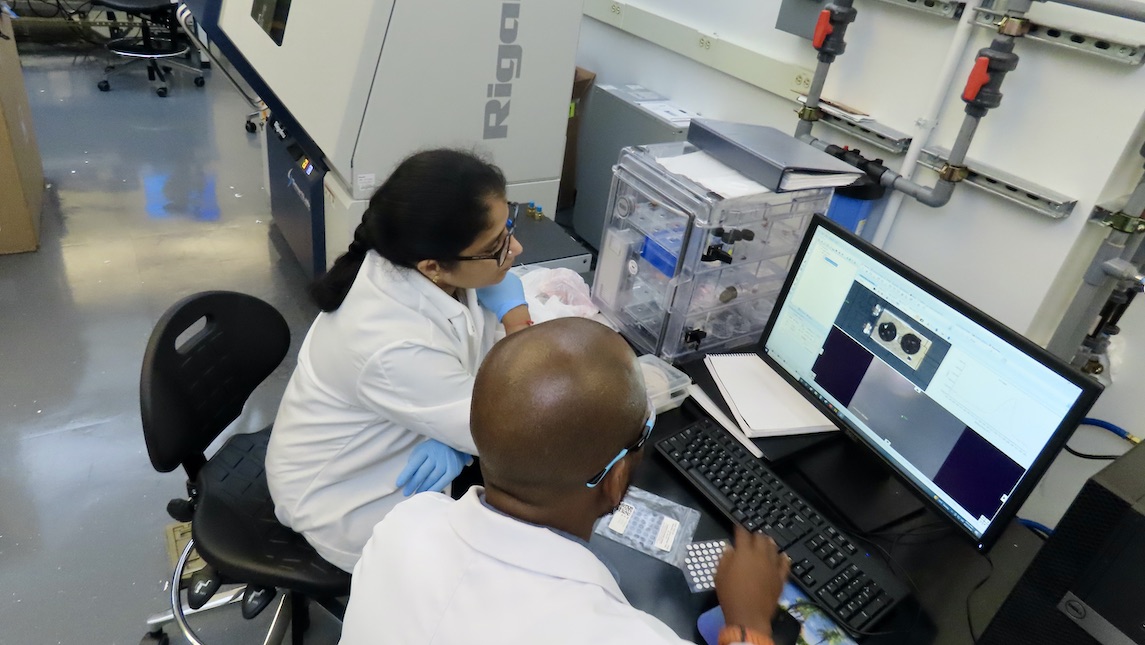

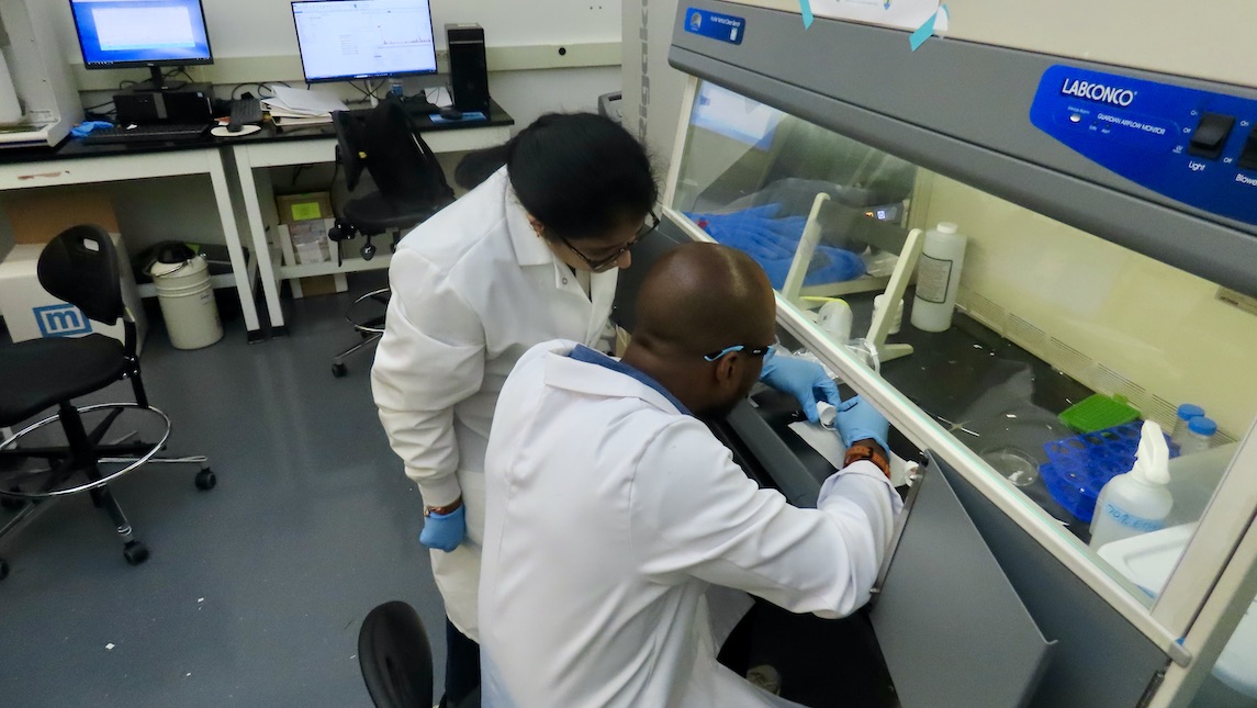
At JSNN, students operate the instrument, interpret surface-chemistry data, and link their findings directly to material performance, gaining technical skills that prepare them for careers in microelectronics, energy, and materials engineering. External academic partners access XPS data to validate experimental findings, explain material behaviors, and support high-impact research journal publications.
Together, these technologies give JSNN students opportunities to develop advanced research skills while providing academic and industry partners access to specialized capabilities that accelerate discovery. From understanding living cells to engineering materials at the nanoscale, JSIRT extends the reach of nanoscience research at JSNN and beyond.
“Whether we are helping a student learn a new technique or a company solve a technical challenge, we turn ideas into discoveries and prepare the next generation of scientists and engineers,” Aravamudhan says.
Written by Amy Burtch, AMBCopy
Photos provided by Joint School of Nanoscience and Nanoengineering